As part of the effort to create our clock-and-scoring box for our fencing club, we're creating our own circuit boards. We've broken the system up into a series of small functions, and we're doing one board for each function. One of the boards we have to do is the keypad.
Most of the boards so far have been done by Mark; but the keypad is mine. Partly I'm doing the board because it makes sense: I'm the one who is developing the software for the keypad, so I know exactly what's required, and I'm the one who built the initial prototype. But partly I'm doing it because I've never printed my own board before, and it's something I want to try.
On a number of occasions, I've used some kind of strip board to construct some project or other. (This was how I did the proto keypad.) When you're using these, you buy a board pre-made with regular strips of copper, and regular patterns of holes drilled in those copper strips. You solder in your components, add wire links as necessary, and cut tracks as necessary. In some circumstances, this can produce quite an elegant result; but it's not particularly durable, and there's a certain maximum complexity you can attain before things just start to get really icky, with wires running over and under each other every which way. My proto keypad attained this level of ickyness after I'd added 14 of its planned 20 keys. But it worked with those keys, and formed an adequate platform for developing the software.
This board is the next step beyond. I know what general layout I want, because I figured all that out while doing the proto. I take my laptop with me to Queensland, and start doing up artwork for the board using Paint Shop Pro. Now, if you're wealthy, then you'll own some sort of CAD/CAM package specifically designed for dealing with circuit boards. All you do is place the components on the board, tell it what connects where, and it will deal with routing the actual copper tracks on the board. But if you're down at the more poverty-stricken end of the market, like me, you use whatever comes to hand. And what comes to my hand is trusty old Paint Shop.
Again, if you're wealthy, you can use a double-sided board. This makes routing a doddle, because you can have copper tracks on both sides of the board, and little tunnels called "vias" connecting them. Whenever two tracks want to cross, one just tunnels through to the other side of the board for a while. But once again, this is beyond our means: printing your own double-sided boards is a bitch, because the trackwork on the two sides have to be aligned perfectly. So we're stuck in single-sided land, which means that if two tracks want to cross, you try and find a twisty-turny way to work them around each other, and if that doesn't work, you have to add a wire link to the top of the board.
The artwork takes considerable time. Much of this time is due to my perfectionism.
Finally, I manage to produce some artwork that fits the 20 buttons, 6 resistors, 4 diodes, 3 LEDs, 3 capacitors, 2 chips, an RJ12 socket and a crystal into the available 16cm by 8 cm space. It needs 11 wire links.
My initial plan was that I would take my artwork over to Mark's, where we could print it out on transparency on his laser printer, and where he could oversee my manufacture of the board; him having done this before, and all. We run into only two problems: Mark's printer is out of toner, and Mark is out of unprinted boards. Mark alerts me as to the existence of transparency film for inkjet printers (something hitherto unknown to me). I buy some, and also buy an unprinted board from RadSpares.
The board from RadSpares is big enough to fit two of my keypad boards plus some space left over for test runs; in other words, I get two chances to get this right.
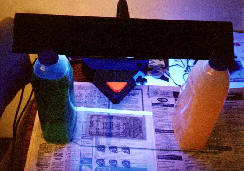
Mark had a tiny scrap of unprinted board left over, and I use this to learn about the process. I print out my artwork on transparency, and set up the scrap of unprinted board under the UV lamp.
Unprinted board consists of the board itself, which is a sort of fibreglassy material, covered by a solid layer of copper, covered by a layer of photoresist, covered by a sticky film to protect it from light. I peel off the protective film, lay it under the UV lamp, and lay the artwork on top. Exposure time under the lamp is a variable (i.e. Mark can't remember how long it should be), but I try three minutes.
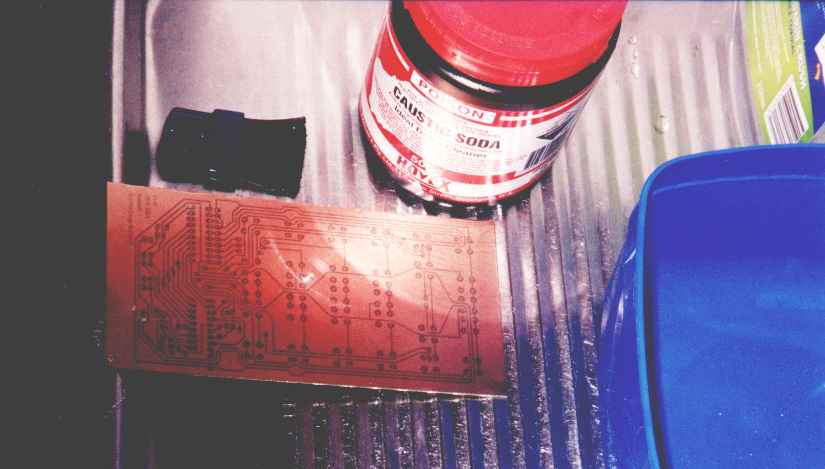
Then I turn off the lamp, take the board over to the sink, and drop it in caustic soda. Caustic soda, aka sodium hydroxide, aka drain cleaner, is used to develop the photoresist. This is extremely cool to watch: initially, the unexposed places where you want to end up with copper are just marginally darker than the exposed places where you want the copper eaten away. When you drop it in the sodium hydroxide, over a period of about five seconds the exposed areas turn a dark purple. Then, over the next couple of minutes, the dark purple areas of the photoresist get eaten away, and you're left with the unexposed bits of the photoresist still stuck to the board, and the exposed areas eaten away, leaving bare copper, ready for the next stage.
At least, that's what's supposed to happen. In my case, some of the unexposed photoresist has been eaten, and some of the unexposed hasn't. But it's still more or less OK.
The next stage is ferric chloride, or as we like to call it, ammonium persulphate. This eats away the exposed copper, leaving behind only the copper protected by the photoresist. The challenge here is that the reaction only starts working at about 70 degrees C, so the water in which the persulphate is dissolved needs to be really hot. I start by boiling some water on the stove, pouring the water into a plastic tub, then pouring in the persulphate, stirring until it dissolves, then dropping in the board. During this whole process the water has cooled, so despite my intensely staring at the board, nothing happens.
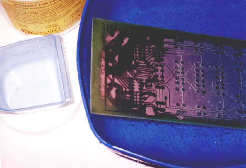
Procedure at this point is to stick it in the microwave for a couple of minutes.
Two minutes later, the reaction is chugging along nicely. Little bubbles of some unknown (but hopefully harmless) gas are forming on the board. Every time a bubble takes off and swims to the surface, it leaves behind a tiny pit that contains less copper than it used to. The regions of board under attack go pale pink, and the water goes blue. The pale regions expand, as more and more copper gets attacked, and then shrink, as the copper gets eaten completely away exposing bare board underneath.
What I'm left with is a board that more or less has copper where I wanted it, and more or less doesn't have copper where I didn't want it. In actual fact, the copper tracks are pitted, and the region between tracks contains many tiny spots of copper. In several places these spots are large enough and numerous enough to cause short circuits between tracks.
A phone conversation with Mark suggests that these problems might well be a combination of insufficient exposure time under the UV lamp, and the scrap of board being rather old.
So I cut a piece of fresh board to the size of the keypad, and give it a try. The five minute exposure under the UV lamp seems to go fine, but the developing in the sodium hydroxide doesn't work. The exposed regions go purple, as they should, but they don't get eaten away. I try brushing away the purple with a small brush, but I wind up also brushing away the undeveloped regions of photoresist, and so end up with a perfectly clean rectangle of solid copper.
A further phone conversation with Mark suggests that the problem may now be too long an exposure time. I print three copies of some 3cm by 3cm board artwork, and expose them onto a piece cut off my remaining unprinted board, for three, four and five minutes. All three develop perfectly. All three etch perfectly.
So I try again with another full-size piece. I get the same result: the photoresist turns dark purple, but doesn't get etched away. Again, I attempt to brush away the purple, and wind up brushing off all the photoresist.
So small boards etch perfectly, but large boards don't. Hmm.
Lying awake in bed at midnight, I am struck by inspiration: I'm not using enough water. The sodium hydroxide is easily soluble in water (in fact, it's deliquescent: in the solid form it will rip water vapour right out of the air in order to have something to dissolve in), but the polymer photoresist is not so soluble. So a small amount of the polymer is initially dissolving, but the rest is sitting right where it started, on the board.
In the morning, I nip out to RadSpares and buy another board. This time I use more water, and the developing process goes perfectly: the exposed regions of board turn purple, and then eventually go pale pink, as the bare copper shows through.
The ammonium persulphate stage is a little challenging. The only microwaveable container I have big enough to hold the 16cm long board is a 2-litre ice-cream tub. And the board only just fits: it has to go in on a diagonal, so in order to completely cover the board with water, the tub must be full to the brim. This makes it something of a challenge to get in and out of the microwave without spilling any of the solution, and without melting my hands. I put the tub in, run the microwave for two minutes, pull it out, look in vain for bubbles, put it back in for another two minutes, and repeat. It takes 20 minutes of microwave time to adequately heat the water. It's nerve-wracking, because while the tub is in the microwave, I can't see what's going on, and even when I've got it out for inspection, and can see the reaction proceeding, I still don't know whether all the copper I want etched is going to etch, and whether all the copper I want to keep will in fact be kept.
Nevertheless, the board does etch exactly the way I want. I solder on the 50 components and wire links, and meet with Mark to test it. It works first try.